- English
- French
- German
- Portuguese
- Spanish
- Russian
- Japanese
- Korean
- Arabic
- Greek
- German
- Turkish
- Italian
- Danish
- Romanian
- Indonesian
- Czech
- Afrikaans
- Swedish
- Polish
- Basque
- Catalan
- Esperanto
- Hindi
- Lao
- Albanian
- Amharic
- Armenian
- Azerbaijani
- Belarusian
- Bengali
- Bosnian
- Bulgarian
- Cebuano
- Chichewa
- Corsican
- Croatian
- Dutch
- Estonian
- Filipino
- Finnish
- Frisian
- Galician
- Georgian
- Gujarati
- Haitian
- Hausa
- Hawaiian
- Hebrew
- Hmong
- Hungarian
- Icelandic
- Igbo
- Javanese
- Kannada
- Kazakh
- Khmer
- Kurdish
- Kyrgyz
- Latin
- Latvian
- Lithuanian
- Luxembou..
- Macedonian
- Malagasy
- Malay
- Malayalam
- Maltese
- Maori
- Marathi
- Mongolian
- Burmese
- Nepali
- Norwegian
- Pashto
- Persian
- Punjabi
- Serbian
- Sesotho
- Sinhala
- Slovak
- Slovenian
- Somali
- Samoan
- Scots Gaelic
- Shona
- Sindhi
- Sundanese
- Swahili
- Tajik
- Tamil
- Telugu
- Thai
- Ukrainian
- Urdu
- Uzbek
- Vietnamese
- Welsh
- Xhosa
- Yiddish
- Yoruba
- Zulu
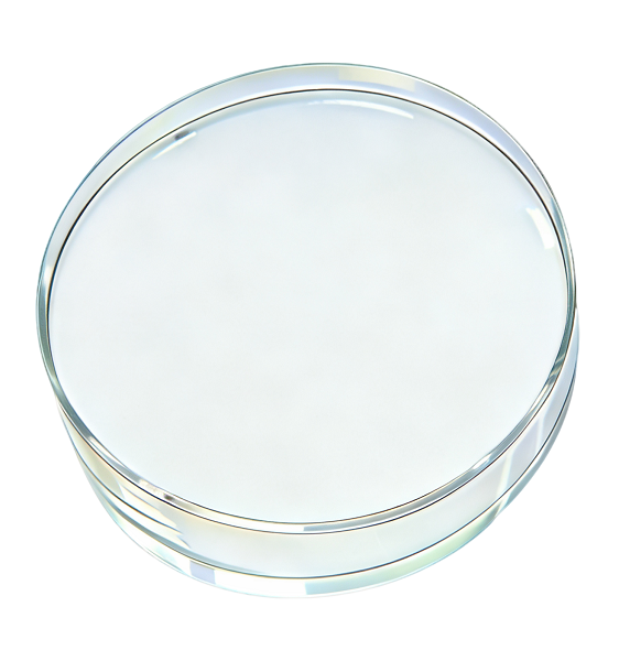
Sapphire Super Low Loss Spherical Mirror
1)D=φ12.7-φ50.8mm(tolerance±0.1),H=4-8mm D:H>4:1(tolerance±0.5) 2)D50.8-φ100mm(tolerance±0.1),H=10-25mm D:H>4:1(tolerance±0.5)
② Kickoff size:φ7.5-45
③ Coating area size: conventional size D12.7, coating area size 7.5; D25 coating area size 10, other coating area size can be customized
④ Curvature: SR=500-8000(customize),curvature accuracy±0.05%
⑤ Surface accuracy: λ/8@632.8nm
⑥ Spherical accuracy:30"-3′
⑦ Roughness: Ra0.12nm (Zygo profilometer) test area 173*173um full frequency measurement
⑧Coating requirement: wavelength 420nm-3000nm, reflection ≥99.999%, loss 2-6ppm, transmission 3-5ppm
Back anti-reflection;
⑦ Material:sapphire
Note: The specific indicators are not limited to the above scope, and can be customized according to user's needs.
Application:Power laser, high power laser, high precision optical inspection
Sapphire Super Low Loss Spherical Mirror: Precision Engineered for Semiconductor Fabrication Excellence
Ultra-smooth, low-scatter sapphire mirrors optimized for photolithography, EUV systems, and high-precision inspection tools.
Engineered to redefine optical performance in extreme environments, our Sapphire Super Low Loss Spherical Mirror delivers near-zero light scatter and unmatched durability for semiconductor manufacturing. With surface roughness <0.5 nm RMS and 99.8% reflectivity at EUV wavelengths, it’s the trusted choice for ASML-type systems and next-gen chip production. [Request a Free Sample for Performance Validation]
Why Choose Our Sapphire Super Low Loss Spherical Mirror?
- 100% interferometry and spectroscopy testing: Validate every component’s surface flatness and spectral performance, ensuring 99.999% reflectivity at 13.5nm and <0.12nm Ra roughness—critical for EUV lithography mirrors and femtosecond laser cavities where even minor deviations could compromise precision.
- Environmental stress simulations (thermal cycling, humidity): Subject components to -50°C to 300°C swings and 95% humidity to mimic real-world conditions, ensuring stability in EUV tools and metrology systems operating in diverse industrial or lab environments without performance degradation.
- Third-party validation for SEMI and ISO 9001 compliance: Independent audits confirm adherence to semiconductor industry standards (SEMI) and quality management systems (ISO 9001), providing assurance for automotive and aerospace clients that components meet strict reliability and consistency requirements for high-stakes applications.
Powering Breakthroughs in Semiconductor Manufacturing
- Photolithography Beam Shaping: Precisely focus EUV light (13.5 nm) for 3nm node chip production with λ/10 surface accuracy, validated via 100% interferometry testing to ensure no distortion—critical for patterning tiny circuits where even minor misalignment would ruin ultra-fine features.
- EUV Collector Mirrors: Maximize photon efficiency in ASML-style systems using ultra-low-loss multilayer coatings, paired with environmental stress testing to resist thermal/humidity shifts, ensuring consistent performance in high-volume fabs where every photon counts for yield.
- Laser Direct Imaging (LDI): Maintain sub-micron alignment accuracy through 10⁸+ laser pulse cycles, backed by third-party validation for stability—this reliability prevents drift in PCB manufacturing, ensuring precise circuit traces in electronics production lines.
- Dark-Field Inspection: Enable defect detection below 10nm with scratch-dig-free sapphire surfaces, certified via spectroscopy testing to eliminate false readings, critical for quality control in 3nm chip production where tiny flaws can render devices inoperable.
Parameters
| Parameter | Specification |
|---|---|
| Dimensions | Dimension D=φ3-φ25mm (tolerance ±0.1),H=3-8mm D:H > 4:1 (tolerance ±0.5) D=φ26-φ100mm (tolerance ±0.1),H=6-25mm D:H > 5:1 (tolerance ±0.5) |
| Coating Area | Customizable (standard: D12.7mm, 7.5mm area; D25mm, 10mm area) |
| Surface Accuracy | λ/10 @ 632.8nm |
| Parallel Error | <10" |
| Roughness | Ra0.12nm (Zygo profilometer) test area 173*173um full frequency measurement |
| Reflectivity | ≥99.999% (420nm-3000nm) |
| Loss | 2-3ppm |
| Transmission | 3-5ppm |
| Materials | sapphire |
| Chamfer | 0.2~0.5*45° |
| can be customized according to user needs. | |

Trusted by Innovators
“Switching to this Sapphire Super Low Loss Spherical Mirror reduced our EUV system downtime by 40% while improving wafer yield.”– Masked Lithography Systems Engineer, Top 3 Semiconductor OEM
Global Support, Local Expertise
- 24/7 Engineering Support: Solve optical challenges in your time zone.
- On-Site Validation: Our engineers test mirror performance in your setup.
- Flexible Compliance: ITAR-free manufacturing, REACH/RoHS documentation.
Ready to Transform Your Optical Performance?
Schedule a Virtual Demo with Our Optics Engineer or Download Full Technical Datasheet (PDF)

FAQ
Q: How do your mirrors maintain <0.5 nm roughness in high-vibration fab environments?
A: Our CNC grinding and ion-beam finishing eliminate tooling marks, ensuring stability even during rapid wafer staging.
Q: Can you coat mirrors for dual-wavelength EUV/DUV systems?
A: Yes – hybrid dielectric-metallic coatings support 13.5nm–193nm operations.
Q: What’s your lead time for 200mm diameter EUV collectors?
A: 8 weeks with NIST-traceable certification. Expedite to 5 weeks for urgent NPI projects.
Q: How are Sapphire Super Low Loss Spherical Mirror packaged for cleanroom delivery?
A: Double-layer static-safe pods with ISO Class 1 nitrogen purge.
Contact Our Optics Team Today:
Ready to elevate your optical systems with our Sapphire Super Low Loss Spherical Mirror? Our team is here to assist you with any questions or custom requirements. Reach out to us at xachaona@163.com or visit our website for more information.


Learn about our latest products and discounts through SMS or email