- English
- French
- German
- Portuguese
- Spanish
- Russian
- Japanese
- Korean
- Arabic
- Greek
- German
- Turkish
- Italian
- Danish
- Romanian
- Indonesian
- Czech
- Afrikaans
- Swedish
- Polish
- Basque
- Catalan
- Esperanto
- Hindi
- Lao
- Albanian
- Amharic
- Armenian
- Azerbaijani
- Belarusian
- Bengali
- Bosnian
- Bulgarian
- Cebuano
- Chichewa
- Corsican
- Croatian
- Dutch
- Estonian
- Filipino
- Finnish
- Frisian
- Galician
- Georgian
- Gujarati
- Haitian
- Hausa
- Hawaiian
- Hebrew
- Hmong
- Hungarian
- Icelandic
- Igbo
- Javanese
- Kannada
- Kazakh
- Khmer
- Kurdish
- Kyrgyz
- Latin
- Latvian
- Lithuanian
- Luxembou..
- Macedonian
- Malagasy
- Malay
- Malayalam
- Maltese
- Maori
- Marathi
- Mongolian
- Burmese
- Nepali
- Norwegian
- Pashto
- Persian
- Punjabi
- Serbian
- Sesotho
- Sinhala
- Slovak
- Slovenian
- Somali
- Samoan
- Scots Gaelic
- Shona
- Sindhi
- Sundanese
- Swahili
- Tajik
- Tamil
- Telugu
- Thai
- Ukrainian
- Urdu
- Uzbek
- Vietnamese
- Welsh
- Xhosa
- Yiddish
- Yoruba
- Zulu
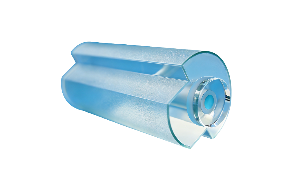
Single Crystal Silicon Super Low Loss Spherical Mirror
1)D=φ12.7-φ50.8mm(tolerance±0.1),H=4-8mm D:H>4:1(tolerance±0.5) 2)D50.8-φ100mm(tolerance±0.1),H=10-25mm D:H>4:1(tolerance±0.5)
② Kickoff size:φ7.5-45
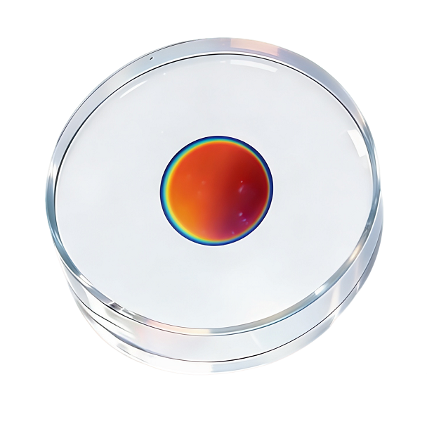
③ Coating area size: conventional size D12.7, coating area size 7.5; D25 coating area size 10, other coating area size can be customized
④ Curvature: SR=500-8000(customize),curvature accuracy±0.05%
⑤ Surface accuracy: λ/2-λ/10@632.8nm
⑥ Spherical accuracy:30"-3′
⑦ Roughness: Ra0.12nm (Zygo profilometer) test area 173*173um full frequency measurement
⑧Coating requirement: wavelength 632nm-1550nm, reflection ≥99.999%, loss 2-6ppm, transmission 3-5ppm
Back anti-reflection;
⑦ Material:single crystal silicon
Note: The specific indicators are not limited to the above scope, and can be customized according to user's needs.
Single Crystal Silicon Super Low Loss Spherical Mirror for Precision EUV Systems
Engineered to achieve <0.1 nm surface roughness and 99.9999% material purity, our Single Crystal Silicon Super Low Loss Spherical Mirror redefines optical precision for extreme ultraviolet (EUV) lithography, quantum computing, and aerospace systems. With vertically integrated manufacturing from crystal growth to ISO-certified metrology, we deliver mirrors that maintain λ/10 surface accuracy even under 500K thermal loads.

Parameters
| Parameter | Specification |
|---|---|
| Dimension | 1)D=φ12.7-φ50.8mm(tolerance±0.1),H=4-8mm D:H>4:1(tolerance±0.5) 2)D50.8-φ100mm(tolerance±0.1),H=10-25mm D:H>4:1(tolerance±0.5) |
| Kickoff size | φ7.5-45mm |
| Coating area | conventional size D12.7, coating area size 7.5; D25 coating area size 10, other coating area size can be customized |
| Curvature | SR: 500-8000mm (customizable), accuracy ±0.05% |
| Surface accuracy | λ/2-λ/10 @632.8nm |
| Spherical accuracy | 30"-3' |
| Roughness | Ra0.12nm (Zygo profilometer) test area 173*173um full frequency measurement |
| Coating | R ≥ 99.999%, loss 2-6ppm, T: 3-5ppm (632-1550nm) |
| Material | Single crystal silicon |
| Chamfer | 0.2~0.5*45° |
| can be customized according to user needs. | |
Why Our Mirrors Outperform
Atomic-Level Surface Perfection
- Sub-ångström smoothness: Achieve ≤0.12 nm Ra roughness via magnetorheological finishing, eliminating light scatter in EUV lithography and dark-field inspection—critical for 3nm chip production where even atomic-scale irregularities would distort 13.5nm light, ensuring flawless patterning and defect detection.
- Zero subsurface damage: Stress-free polishing prevents laser-induced fractures, vital for EUV collector mirrors and LDI systems, where material stress could cause catastrophic failure under high-power pulses, maintaining integrity through 10⁸+ cycles in semiconductor fabs.
- Crystallographic uniformity: <0.1° orientation deviation across entire surface ensures consistent optical properties, key for photolithography beam shaping and inspection tools—this uniformity prevents localized performance drops, critical for reliable 3nm node manufacturing and high-precision defect analysis.
EUV-Optimized Performance
- 95%+ reflectivity at 13.5 nm wavelength: Ensures maximal photon utilization in EUV lithography for 3nm chip production, where every 13.5nm photon is critical for precise patterning—this high reflectivity minimizes energy loss, boosting throughput in semiconductor fabs reliant on efficient light usage.
- <5 ppm absorption loss even at 20 W/cm² EUV flux: Prevents excessive heating and performance degradation in high-power EUV systems, maintaining stability in collector mirrors and beam shapers under intense flux, crucial for avoiding thermal distortion that would ruin 3nm node circuit patterns.
- 0.05 ppm/K thermal expansion stability: Guarantees dimensional consistency across temperature fluctuations in EUV tools, ensuring alignment accuracy in photolithography and inspection systems—this stability prevents misalignment that could compromise 3nm manufacturing precision, even as operational temperatures vary.
Mission-Critical Reliability
- 10-year lifespan under 24/7 high-energy operation: Ensures long-term reliability in EUV lithography systems running continuously, reducing downtime for replacements in 3nm chip fabs—this durability matches the high reflectivity and low absorption, maintaining consistent performance through years of intense 13.5nm photon exposure.
- MIL-O-13830A compliant shock/vibration resistance: Withstands mechanical stress in transport and operation, critical for EUV tools moved between facilities or exposed to factory vibrations, preventing alignment shifts that would disrupt 3nm patterning, complementing thermal stability for all-around robustness.
- Custom AR coatings to suppress 632-1550 nm back reflections: Eliminates interference from stray wavelengths in multi-system setups, ensuring 13.5nm EUV light remains uncompromised—this precision enhances photolithography accuracy, pairing with low absorption to optimize 3nm node manufacturing efficiency.
Precision Engineered for 3nm Chip Production
Our Single Crystal Silicon Super Low Loss Spherical Mirror enables next-gen semiconductor manufacturing by:
1. Eliminating pattern distortion through λ/20 wavefront accuracy
2. Reducing mirror replacement cycles by 40% via defect-free surfaces
3. Maintaining beam coherence with <0.001% thermal drift at 500K
Trusted by Global Innovators
"After switching to their Spherical Mirrors, we achieved 1.8% higher wafer yields in our 5nm node production line."– Chief Engineer, Top 3 Semiconductor OEM
Customization & Compliance
- Size Flexibility: From φ7.5 mm micro-optics to 100 mm substrates
- Coating Options:
- Broadband UV-IR (250-2000 nm)
- Narrow-linewidth laser (±0.1 nm)
- EUV-optimized multilayer stacks
- Certifications:
- ISO 9001/14001 certified production
- ITAR-free, REACH/ROHS compliant
- Full ASML supplier audit readiness

FAQs
Q: How do you prevent thermal deformation in high-power applications?
A: Our mirrors leverage single-crystal silicon's ultra-low CTE (0.05 ppm/K) combined with stress-free mounting designs, limiting shape deviation to <1 nm even at 500K.
Q: What quality control measures ensure defect-free surfaces?
A: Every Single Crystal Silicon Super Low Loss Spherical Mirror undergoes:
- White light interferometry (0.1 nm resolution)
- 100% defect mapping via dark-field microscopy
- LIDT testing to 50 MW/cm²
Q: Can you match existing OEM coating specifications?
A: Yes. Share your reflectivity curve requirements, and our coating team will provide loss-optimized solutions within 72 hours.
Request Your Free Mirror Simulation
Ready to elevate your optical systems with our Single Crystal Silicon Super Low Loss Spherical Mirror? Our team of experts is here to assist you in finding the perfect solution for your project.
Email: xachaona@163.com


Learn about our latest products and discounts through SMS or email