- English
- French
- German
- Portuguese
- Spanish
- Russian
- Japanese
- Korean
- Arabic
- Greek
- German
- Turkish
- Italian
- Danish
- Romanian
- Indonesian
- Czech
- Afrikaans
- Swedish
- Polish
- Basque
- Catalan
- Esperanto
- Hindi
- Lao
- Albanian
- Amharic
- Armenian
- Azerbaijani
- Belarusian
- Bengali
- Bosnian
- Bulgarian
- Cebuano
- Chichewa
- Corsican
- Croatian
- Dutch
- Estonian
- Filipino
- Finnish
- Frisian
- Galician
- Georgian
- Gujarati
- Haitian
- Hausa
- Hawaiian
- Hebrew
- Hmong
- Hungarian
- Icelandic
- Igbo
- Javanese
- Kannada
- Kazakh
- Khmer
- Kurdish
- Kyrgyz
- Latin
- Latvian
- Lithuanian
- Luxembou..
- Macedonian
- Malagasy
- Malay
- Malayalam
- Maltese
- Maori
- Marathi
- Mongolian
- Burmese
- Nepali
- Norwegian
- Pashto
- Persian
- Punjabi
- Serbian
- Sesotho
- Sinhala
- Slovak
- Slovenian
- Somali
- Samoan
- Scots Gaelic
- Shona
- Sindhi
- Sundanese
- Swahili
- Tajik
- Tamil
- Telugu
- Thai
- Ukrainian
- Urdu
- Uzbek
- Vietnamese
- Welsh
- Xhosa
- Yiddish
- Yoruba
- Zulu
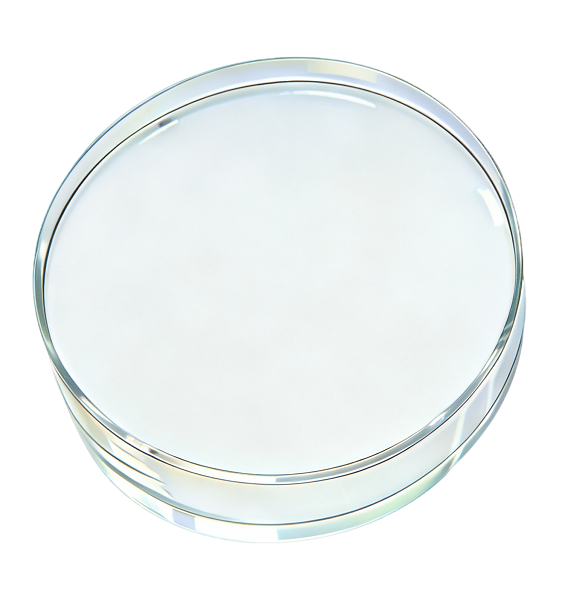
Fused Silica Mirror Substrate
②Surface accuracy: λ/2-λ/ 10@632.8nm
③ Parallel error: <15"
④ Roughness: single-side Ra0.12nm (Zygo profilometer) test area 173*173um full frequency measurement
⑤ Material: ULE, fused silica,zerodur, sapphire, K9, single crystal silicon;
Note: The specific indicators are not limited to the above scope, and can be customized according to user's needs.
Application:Laser gyro, high power laser, superstable laser, high precision optical inspection, semiconductor manufacturing, semiconductor inspection
Fused Silica Mirror Substrate: Precision Engineered for Cutting-Edge Optics
When you need mirror substrates that deliver uncompromising performance in extreme environments, our Fused Silica Mirror Substrate stands as the gold standard. Crafted from ultra-high purity synthetic silica, these substrates excel in EUV lithography, semiconductor inspection, and high-power laser systems where thermal stability (CTE <5 ppb/K) and λ/10 surface flatness are non-negotiable. With 20+ years of expertise in precision optics, we’ve engineered substrates that meet MIL-SPEC, SEMI, and ASML-tier requirements while supporting rapid prototyping and high-volume orders.
Why Our Fused Silica Substrates Outperform
1. Extreme Environment Resilience
- Thermal Stability: Maintains <5 ppb/K expansion from -60°C to 200°C
- Laser Resistance: Withstands >10 J/cm² @ 355nm (ideal for excimer lasers)
- Radiation Hardening: Zero degradation under prolonged EUV/X-ray exposure
2. Atomic-Level Surface Precision
- Sub-Ångström Roughness: Ra <0.5Å verified via AFM
- Nanometer Flatness: Achieves λ/20 over 300mm diameters
- Stress-Free Polishing: Minimizes wavefront distortion
3. Custom-Built for Your Workflow
- Diameter Options: 10mm to 450mm (±0.1mm tolerance)
- Coatings: AR, HR, DLC, or EUV multilayers (13.5nm optimized)
- Edge Profiles: Chamfered, beveled, or metrology-ready
Parameters
| Parameter | Specification |
|---|---|
| Dimension | D=φ10-φ100mm (tolerance ±0.1), H=3-30mm (tolerance ±0.5) |
| Surface Accuracy | λ/2-λ/10@632.8nm |
| Parallel Error | <15" |
| Roughness | Single-side Ra0.12nm (Zygo profilometer), test area 173*173um full frequency measurement |
| Material Options | ULE, fused silica, zerodur, sapphire, K9, single crystal silicon |
Note: Custom specifications available upon request to meet your specific needs.

Where Precision Matters Most
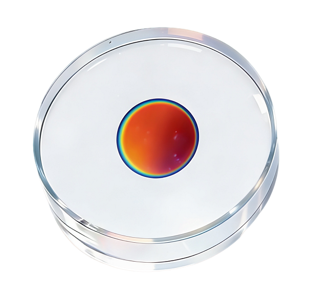
- EUV Lithography Systems: Mirror substrates with <0.1 defects/cm² ensure defect-free wafer patterning at 3nm nodes, a breakthrough for advanced semiconductor manufacturing. This ultra-low defect density prevents pattern distortions during extreme ultraviolet lithography, enabling the production of smaller, more powerful chips that drive next-gen computing and electronics innovation.
- Semiconductor Metrology: λ/40 flatness enables sub-nm measurement accuracy in overlay inspection tools, critical for verifying chip alignment during fabrication. This exceptional flatness ensures precise dimensional checks, helping semiconductor manufacturers maintain strict quality control and meet the tight tolerances required for high-performance microchips.
- High-Power Laser Optics: Boasting a 5x higher laser damage threshold vs. standard fused silica, these optics excel in high-intensity laser systems. They withstand extreme energy levels without degradation, making them ideal for industrial cutting, military directed energy applications, and scientific research where reliable performance under intense power is paramount.
- Space & Defense Optics: Radiation-hardened grades survive LEO/GEO orbital conditions, enduring cosmic radiation and extreme temperature swings. These optics maintain stability in satellite sensors, missile guidance systems, and space telescopes, ensuring consistent performance in the harsh environment of space and critical defense operations.
Quality Assured, Every Time
- 100% Surface Inspection: Zygo GPI-XP & Bruker AFM validation
- Traceability: Lot-specific certs with CTE/OH⁻ content data
- Compliance: ISO 9001, IATF 16949, SEMI F57
Tailored to Your Exact Needs
Whether you need:
- Prototypes: 6-week turnaround for R&D samples
- High Volumes: 10,000+ substrates/month capacity
- Hybrid Designs: Pre-mounted or pre-coated configurations
Our engineers work directly with your team to optimize edge exclusion zones, mounting interfaces, and thermal deformation models.
Trusted by Global Leaders
“After switching to their fused silica mirror substrate, our EUV tool alignment errors dropped by 37%.”
– Optical Engineer, Top 3 Semiconductor OEM
Get Started Today
Download: [Fused Silica Substrate Datasheet] | [SEMI Compliance Report]
Need a Custom Solution?
Email xachaona@163.com for:
- Urgent quotes (<24h response)
- Coating design consultations
- NDA-protected project reviews

FAQ: Your Top Questions Answered
Q: What’s your max substrate size?
A: We regularly produce 800mm-diameter substrates with <λ/10 flatness.
Q: Do you test EUV reflectance?
A: Yes – we provide 13.5nm reflectivity maps measured at PTB/BESSY II.
Q: How do you prevent shipping damage?
A: Triple-layer packaging (VCI film, desiccant, hard cases) with shock sensors.
Q: Can you match OEM drawings?
A: We’ve qualified substrates for 7/10 top semiconductor OEMs – send your specs.
Q: What about contamination control?
A: Our cleanrooms outperform ISO 14644-1 Class 5 standards.
Contact us
When your optical systems demand substrates that balance atomic-level precision with industrial durability, our Fused Silica Mirror Substrate solutions deliver. Contact xachaona@163.com to discuss your project – let’s build the foundation for your next breakthrough.


Learn about our latest products and discounts through SMS or email