- English
- French
- German
- Portuguese
- Spanish
- Russian
- Japanese
- Korean
- Arabic
- Greek
- German
- Turkish
- Italian
- Danish
- Romanian
- Indonesian
- Czech
- Afrikaans
- Swedish
- Polish
- Basque
- Catalan
- Esperanto
- Hindi
- Lao
- Albanian
- Amharic
- Armenian
- Azerbaijani
- Belarusian
- Bengali
- Bosnian
- Bulgarian
- Cebuano
- Chichewa
- Corsican
- Croatian
- Dutch
- Estonian
- Filipino
- Finnish
- Frisian
- Galician
- Georgian
- Gujarati
- Haitian
- Hausa
- Hawaiian
- Hebrew
- Hmong
- Hungarian
- Icelandic
- Igbo
- Javanese
- Kannada
- Kazakh
- Khmer
- Kurdish
- Kyrgyz
- Latin
- Latvian
- Lithuanian
- Luxembou..
- Macedonian
- Malagasy
- Malay
- Malayalam
- Maltese
- Maori
- Marathi
- Mongolian
- Burmese
- Nepali
- Norwegian
- Pashto
- Persian
- Punjabi
- Serbian
- Sesotho
- Sinhala
- Slovak
- Slovenian
- Somali
- Samoan
- Scots Gaelic
- Shona
- Sindhi
- Sundanese
- Swahili
- Tajik
- Tamil
- Telugu
- Thai
- Ukrainian
- Urdu
- Uzbek
- Vietnamese
- Welsh
- Xhosa
- Yiddish
- Yoruba
- Zulu
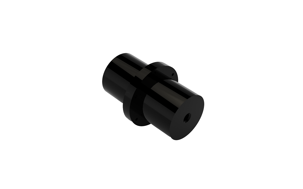
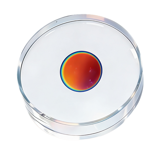
Double Side Super Smooth Flat Mirror Substrate
②Surface accuracy: λ/2-λ/ 10@632.8nm
③ Parallel error: <15"
④ Roughness: double-side Ra0.12nm (Zygo profilometer) test area 173*173um full frequency measurement
⑤ Material: ULE, fused silica,zerodur, sapphire, K9, single crystal silicon;
Note: The specific indicators are not limited to the above scope, and can be customized according to user's needs.
Application:Laser gyro, high power laser, semiconductor manufacturing, semiconductor inspection
Double Side Super Smooth Flat Mirror Substrate | Precision for Micro/Nano-Scale Fabrication
Engineered for perfection in semiconductor lithography, wafer inspection, and advanced display technologies, our Double Side Super Smooth Flat Mirror Substrate delivers sub-Ångström surface roughness and unparalleled flatness (≤0.1μm). Whether you’re tackling nanoscale patterning or high-power laser systems, this substrate ensures defect-free performance with unmatched consistency. Trusted by leading semiconductor OEMs, it’s the backbone of precision where even a single imperfection can cost millions. [Request a Free Sample or Quote]
Key Features That Redefine Precision
- Dual-Side Ultra-Smooth Finish: Achieve Ra ≤0.2Å roughness on both surfaces for flawless light reflection, eliminating wavefront distortion in high-end optics. This exceptional smoothness ensures uniform light transmission, critical for applications like advanced microscopes and lithography systems where even atomic-scale imperfections could compromise performance.
- Thermal & Chemical Stability: Built with fused silica, ULE® glass, or custom ceramics to withstand extreme conditions, resisting thermal expansion and chemical corrosion. Ideal for industrial furnaces, semiconductor etching tools, and harsh-environment sensors, these materials maintain integrity across wide temperature ranges and aggressive chemical exposures.
- Zero Defect Guarantee: Scratch/dig ≤10/5 per MIL-PRF-13830B standards ensures minimal surface flaws, meeting strict military and aerospace quality requirements. This level of perfection prevents light scattering in defense optics and satellite sensors, guaranteeing reliable performance in mission-critical applications where failure is not an option.
- Custom Sizes & Shapes: Diameters from 50mm to 450mm, thicknesses from 0.5mm to 15mm, cater to diverse system designs—from compact laser modules to large telescope mirrors. This versatility allows seamless integration, reducing assembly complexity and optimizing optical performance in both small-scale devices and industrial-grade systems.
- EUV/DUV Compatibility: Optimized for next-gen lithography and metrology systems, these components excel in extreme ultraviolet and deep ultraviolet wavelengths. Their precision ensures accurate light manipulation, enabling the production of 3nm and smaller semiconductor chips, a cornerstone of advanced computing and electronics innovation.
Parameters
| Specification | Value |
|---|---|
| Dimension | D=φ10-φ100mm (tolerance ±0.1), H=3-30mm (tolerance ±0.5) |
| Surface Accuracy | λ/2-λ/10@632.8nm |
| Parallel Error | <15" |
| Roughness | Double-side Ra0.12nm (Zygo profilometer), test area 173*173um full frequency measurement |
| Materials | ULE, fused silica, Zerodur, sapphire, K9, single crystal silicon |
| can be customized according to user needs | |
Note: Custom specifications are available upon request to meet your unique requirements.

Where Precision Meets Innovation
Semiconductor Manufacturing
Eliminate overlay errors in ASML or Nikon scanners with Double Side Super Smooth Flat Mirror Substrate that maintain λ/20 flatness. Perfect for 3nm node processes.
Laser & Optical Systems
Minimize light scattering in high-power lasers or aerospace optics, ensuring beam integrity under stress.
Display Technology
Boost OLED/MicroLED yield rates with large-format substrates (up to 1m²) that resist warping during deposition.
- 100% Inline Inspection: Laser interferometry and Zygo profilometers validate every unit.
- Certified Excellence: ISO 9001, IATF 16949, and SEMI Standards compliance.
- Traceability: Serialized reports for full lot history.
Why Partner With Us?
1. 25+ Years of Expertise: Collaborations with top-tier semiconductor and display manufacturers.
2. R&D-Driven Solutions: Prototype in 15 days with our dedicated engineering team.
3. Sustainable Practices: Eco-friendly production and recyclable packaging options.
Real-World Impact
Case Study 1: Reduced lithography overlay errors by 38% for a leading 3nm node fab.
Case Study 2: Enabled 99.98% defect-free OLED panels for a global display leader.
Flexible Ordering, Global Support
- Volume Discounts: Save on orders of 100+ units.
- Global Shipping: Hassle-free customs documentation included.
- 24/7 Support: Direct access to technical experts.

FAQ: Your Questions, Answered
1. How do you ensure dual-side flatness consistency?
Our proprietary polishing tech and inline metrology guarantee <1µm/m² tolerance.
2. What materials handle high-temperature semiconductor processes?
Fused silica and ULE® glass offer near-zero thermal expansion.
3. Can I get non-standard sizes for R&D projects?
Yes! We specialize in custom dimensions with a 15-day prototype turnaround.
4. How are Double Side Super Smooth Flat Mirror Substrate protected during shipping?
Cleanroom-packed in ISO Class 3 environments with shock-resistant casing.
5. What’s the lead time for 500+ units?
Typically 30 days, with priority scheduling for urgent needs.
Contact Us
Ready to elevate your optical systems with our Double Side Super Smooth Flat Mirror Substrate? Reach out to our team today for quotes, technical discussions, or custom inquiries. Email us at xachaona@163.com or visit our website for more information. Let's work together to bring precision and clarity to your projects!


Learn about our latest products and discounts through SMS or email