- English
- French
- German
- Portuguese
- Spanish
- Russian
- Japanese
- Korean
- Arabic
- Greek
- German
- Turkish
- Italian
- Danish
- Romanian
- Indonesian
- Czech
- Afrikaans
- Swedish
- Polish
- Basque
- Catalan
- Esperanto
- Hindi
- Lao
- Albanian
- Amharic
- Armenian
- Azerbaijani
- Belarusian
- Bengali
- Bosnian
- Bulgarian
- Cebuano
- Chichewa
- Corsican
- Croatian
- Dutch
- Estonian
- Filipino
- Finnish
- Frisian
- Galician
- Georgian
- Gujarati
- Haitian
- Hausa
- Hawaiian
- Hebrew
- Hmong
- Hungarian
- Icelandic
- Igbo
- Javanese
- Kannada
- Kazakh
- Khmer
- Kurdish
- Kyrgyz
- Latin
- Latvian
- Lithuanian
- Luxembou..
- Macedonian
- Malagasy
- Malay
- Malayalam
- Maltese
- Maori
- Marathi
- Mongolian
- Burmese
- Nepali
- Norwegian
- Pashto
- Persian
- Punjabi
- Serbian
- Sesotho
- Sinhala
- Slovak
- Slovenian
- Somali
- Samoan
- Scots Gaelic
- Shona
- Sindhi
- Sundanese
- Swahili
- Tajik
- Tamil
- Telugu
- Thai
- Ukrainian
- Urdu
- Uzbek
- Vietnamese
- Welsh
- Xhosa
- Yiddish
- Yoruba
- Zulu
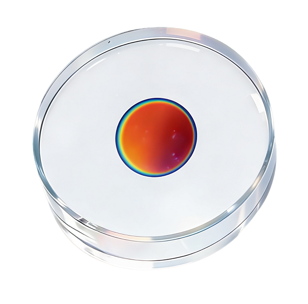
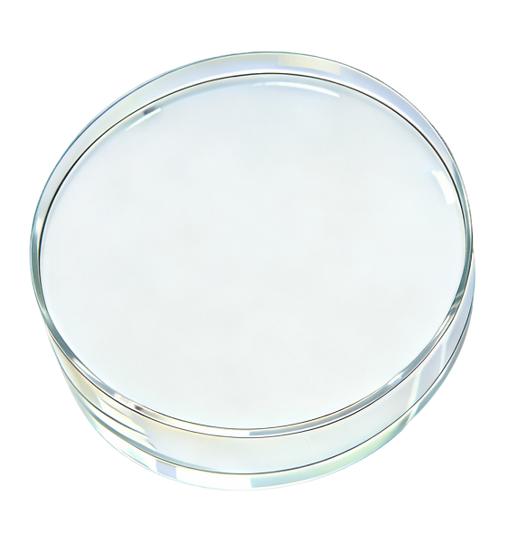
Super Low Expansion Reflective Mirror
D=φ26-φ100mm (tolerance ±0.1),H=6-25mm D:H > 5:1 (tolerance ±0.5)
② Coating area size: conventional size D12.7, coating area size 7.5; D25 coating area size 10, other coating area size can be customized
③ Surface accuracy: λ/ 10@632.8nm
④ Parallel error: <10"
⑤ Roughness: Ra0.12nm (Zygo profilometer) test area 173*173um full frequency measurement
⑥Coating requirement: wavelength 420nm-3000nm, reflection ≥99.999%, loss 2-3ppm, transmission 3-5ppm
Back anti-reflection;
⑦ Material: ULE, fused silica, single crystal silicon, sapphire;
Note: The specific indicators are not limited to the above scope, and can be customized according to user's needs.
Application:Laser gyro, high power laser, super stable laser, high precision optical detection
Why Choose Our Super Low Expansion Reflective Mirror?
When precision matters, our Super Low Expansion Reflective Mirror delivers unmatched performance in the most demanding environments. Designed for semiconductor fabs, aerospace systems, and high-power laser applications, these mirrors combine near-zero thermal expansion with sub-nanometer surface accuracy. Imagine optics that maintain their shape and reflectivity even under rapid temperature swings – that’s what you get with our proprietary glass-ceramic technology.
Core Benefits
- EUV Lithography Machines: Reflect 13.5 nm light with minimal energy loss for sharper wafer patterning, critical for producing 3nm and smaller semiconductor chips. Atomic-level smoothness ensures 99.999% reflectivity, while zero thermal distortion prevents misalignment, boosting yield in high-volume fabs where precision directly impacts production efficiency.
- Laser Wafer Inspection: Detect sub-3nm defects using distortion-free beam steering, enabled by mirrors with <0.5 nm RMS roughness. This precision ensures accurate defect mapping across wafers, helping manufacturers identify flaws early and reduce scrap rates in advanced chip production.
- High-Power Laser Systems: Handle kW-level beams without surface warping or coating damage, thanks to durable multilayer coatings and thermal-stable substrates. These mirrors maintain integrity in 24/7 industrial settings, preventing performance drops in cutting, welding, or material processing applications.
- Space Optics: Withstand orbital thermal swings while maintaining optical alignment, leveraging near-zero CTE materials that resist dimensional changes from -50°C to 150°C. This stability ensures consistent imaging in satellites and telescopes, where thermal-induced misalignment would compromise mission-critical data.
Parameters
| Specification | Value |
|---|---|
| Dimension | D=φ3-φ25mm (tolerance ±0.1),H=3-8mm D:H > 4:1 (tolerance ±0.5) D=φ26-φ100mm (tolerance ±0.1),H=6-25mm D:H > 5:1 (tolerance ±0.5) |
| Coating Area | conventional size D12.7, coating area size 7.5; D25 coating area size 10, other coating area size can be customized |
| Surface Accuracy | λ/10@632.8nm |
| Parallel Error | <10" |
| Roughness | Ra0.12nm (Zygo profilometer) test area 173*173um full frequency measurement |
| Reflection | ≥99.999% (420nm-3000nm) |
| Loss | 2-3ppm |
| Transmission | 3-5ppm |
| Materials | ULE, fused silica, single crystal silicon, sapphire |
| can be customized according to user needs | |

Where It Performs Best
- Semiconductor Lithography: Prevent overlay errors in 3nm chip production with ultra-precise mirrors boasting <0.5nm RMS roughness and near-zero thermal expansion. These components ensure alignment accuracy across repeated exposures, critical for stacking nanoscale circuit layers without misalignment that would ruin yields in high-volume fabs.
- Laser Gyroscopes: Enable drift-free navigation for aerospace systems by maintaining stable beam paths via low-scatter mirrors with <0.1% reflectivity variation. This precision eliminates signal drift caused by optical imperfections, ensuring accurate orientation data for aircraft, satellites, and missile guidance systems.
- Metrology Systems: Measure with atomic-scale precision using mirrors engineered for λ/20 surface accuracy and minimal light scatter. These components enhance interferometer performance, capturing sub-nanometer dimensional changes in semiconductor wafers, optical components, and precision-machined parts.
- High-Power Lasers: Handle kW-level beams without distortion through thermal-stable substrates and robust multilayer coatings. Resisting heat-induced warping and coating degradation, these mirrors maintain beam integrity in industrial cutting, welding, and laser peening applications, ensuring consistent performance in 24/7 operations.
Built to Outlast and Outperform
Every Super Low Expansion Reflective Mirror undergoes:
✅ 100% interferometry inspection
✅ 500-cycle thermal shock testing
✅ Accelerated aging simulations (equivalent to 15 years)
✅ Contamination-controlled packaging (IEST-STD-1246)
“Zero downtime from thermal drift since installing these mirrors.” – Semiconductor Fab Director
3 Reasons We’re the Smart Choice
1. Better Than Fused Silica: 40% lower CTE, 10X smoother surfaces.
2. Proven in Production: Certified suppliers to ASML, Nikon, and TSMC.
3. Sustainable Manufacturing: 95% coating material recycled.

Frequently Asked Questions
Q: How do you maintain defect-free surfaces during coating?
A: Our ion beam sputtering process occurs in ISO Class 1 cleanrooms with real-time thickness monitoring.
Q: What cleaning methods are safe?
A: Use IPA vapor or CO2 snow – we provide detailed protocols with every order.
Q: Can you match legacy system dimensions?
A: Yes! We’ve created custom mirrors for 1980s lithography tools still in operation.
Ready to Upgrade Your Optical Performance?
✅ Free Sample Program: Test a Super Low Expansion Reflective Mirror in your application.
✅ 24/7 Engineering Support: From prototyping to volume orders.
✅ 15-Day Lead Time: With expedited options.
Contact our team today to discuss your requirements:


Learn about our latest products and discounts through SMS or email